19865874889
One stop service platform for electronic components
19865874889
One stop service platform for electronic components

DAC5681IRGCR is a 16-bit 1.0 GSPS digital-to-analog converter (DAC).
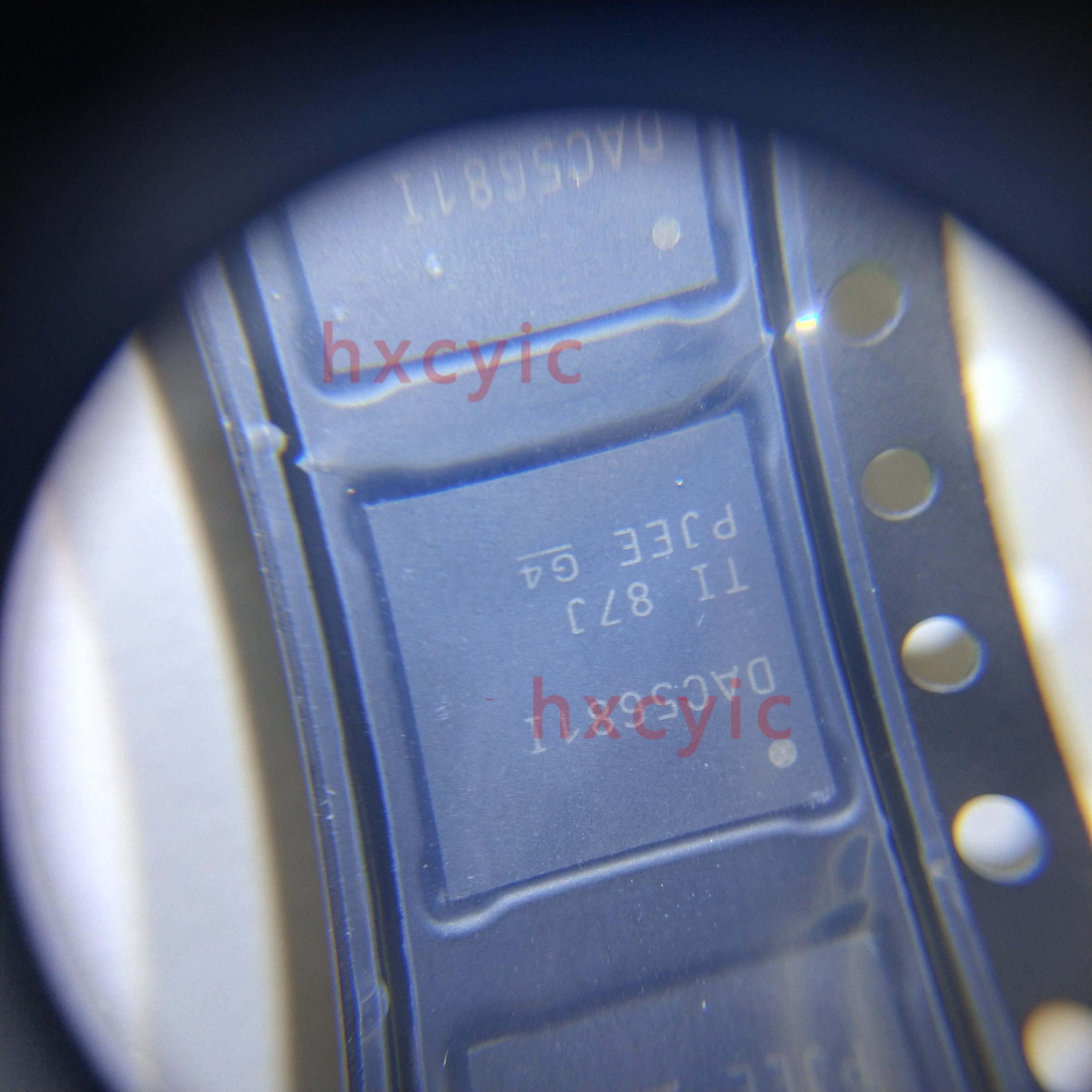
DAC5681 is a 16-bit 1.0 GSPS digital-to-analog converter (DAC) with broadband LVDS data input and internal reference. DAC5681 has excellent linearity and noise performance.
DAC5681 integrates a broadband LVDS port and an on-chip terminal, which can completely transmit 1.0 GSPS data to DAC, and the EMI is lower than that of the traditional CMOS data interface. On-chip delay locked loop (DLL) provides skew control for LVDS input data clock, thus simplifying LVDS interface.
The current steering architecture of DAC5681 consists of a segmented current sink switch array, which can guide the full-scale current up to 20mA to the complementary output node. The accurate on-chip voltage reference can provide a stable 1.2 reference voltage after temperature compensation. You can also choose to use an external reference.
DAC5681 operates over the industrial temperature range of–-40°C to 85°C and is packaged in a 64-lead QFN package. This device can be upgraded to other devices in this series through pins: DAC5681Z and DAC5682Z. Both the single-channel DAC5681Z and the dual-channel DAC5682Z provide optional 2x/4x interpolation and clock multiplication plls.
16-bit digital-to-analog converter (DAC)
1.0 GSPS update rate
16-bit broadband input LVDS data bus
8 samples input FIFO
On-chip delay locked loop
high-performance
73 dBc ACLR WCDMA TM1 at 180 MHz
On-chip 1.2 V reference
Differential scalable output: 2 to 20 mA
Package: 64-lead 9× 9mm QFN
Recommended products
 Complete variety, easy shopping
 Multi warehouse direct shipping, fast delivery
 Authentic goods and exquisite service
 Everyday low prices, worry free selection
-
Phone
19865874889 -
Whatsapp