19865874889
One stop service platform for electronic components
19865874889
One stop service platform for electronic components

K4A4G165WE-BCRC Samsung Electro -Hxcy.IC
2025/7/24 18:02:13
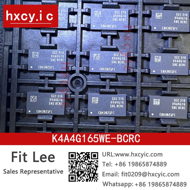
Order Samsung Electro K4A4G165WE-BCRC on Hxcy.IC. Confirm available stock and prices, check the product specifications for K4A4G165WE-BCRC,and place an order online.Contact Email:Fit0209@hxcyic.com
The 4Gb DDR4 SDRAM E-die is organized as a 32Mbitx 16 I/ Os x 8banks device. This synchronous device achieves high speed double-data-rate transfer rates of up to 2400Mb/ sec/ pin (DDR4-2400) for general applica tions.
The chip is designed to comply with the following key DDR4 SDRAM fea tures such as posted CAS, Programmable CWL, Internal (Self) Calibration, On Die Termination using ODT pin and Asynchronous Reset.
All of the control and address inputs are synchronized with a pair of exter nally supplied differential clocks. Inputs are latched at the crosspoint of dif ferential clocks (CK rising and CK falling). All I/ Os are synchronized with a pair of bidirectional strobes(DQS and DQS) in a source synchronous fash ion. The address bus is usẹd to convey row, column, and bank address information in a RAS/CAS miultiplexing style. The DDR4 device operates with a single 1.2V (1.14V~1.26V) power supply,1.2V(1.14V~1.26V) VDDQ and 2.5V (2.375V~2.75V) Vpp.
The 4Gb DDR4 E-die device is available in 96ball FBGAs(x16).
• JEDEC standard 1.2V (1.14V~1.26V)
• VDDQ = 1.2V (1.14V~1.26V)
• VPP = 2.5V (2.375V~2.75V)
• 800 MHz fCK for 1600Mb/sec/pin,933 MHz fCK for 1866Mb/sec/pin,
1067MHz fCK for 2133Mb/sec/pin, 1200MHz fCK for2400Mb/sec/pin
• 8 Banks (2 Bank Groups)
• Programmable CAS Latency(posted CAS):
10,11,12,13,14,15,16,17,18
• Programmable CAS Write Latency (CWL) = 9,11 (DDR4-1600) ,
10,12 (DDR4-1866) ,11,14 (DDR4-2133) and 12,16 (DDR4-2400)
• 8-bit pre-fetch
• Burst Length: 8 , 4 with tCCD = 4 which does not allow seamless read
or write [either On the fly using A12 or MRS]
• Bi-directional Differential Data-Strobe
• Internal(self) calibration : Internal self calibration through ZQ pin
(RZQ : 240 ohm ± 1%)
• On Die Termination using ODT pin
• Average Refresh Period 7.8us at lower than TCASE 85C, 3.9us at
85C < TCASE < 95 C
• Asynchronous Reset
• Package : 96 balls FBGA - x16
• All of Lead-Free products are compliant for RoHS
• All of products are Halogen-free
• CRC(Cyclic Redundancy Check) for Read/Write data security
• Command address parity check
• DBI(Data Bus Inversion)
• Gear down mode
• POD (Pseudo Open Drain) interface for data input/output
• Internal VREF for data inputs
• External VPP for DRAM Activating Power
• PPR is supported
Recommended products
 Complete variety, easy shopping
 Multi warehouse direct shipping, fast delivery
 Authentic goods and exquisite service
 Everyday low prices, worry free selection
-
Phone
19865874889 -
Whatsapp