19865874889
One stop service platform for electronic components
19865874889
One stop service platform for electronic components

ADL5367ACPZ Analog Devices Inc.-Hxcy.IC
2025/7/24 0:20:41
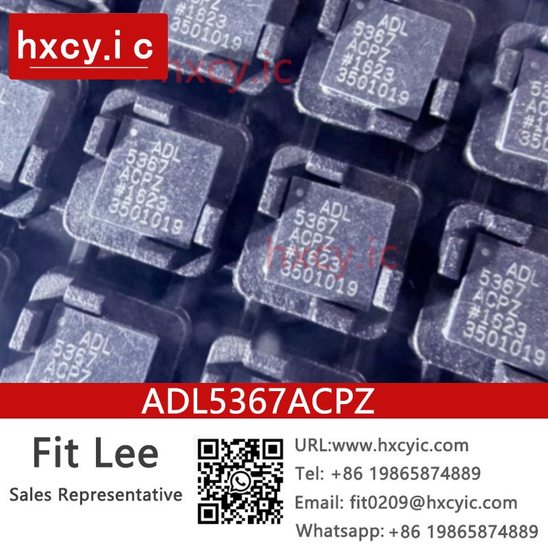
Order Analog Devices Inc. ADL5367ACPZ on Hxcy.IC. Confirm available stock and prices, check the product specifications for ADL5367ACPZ,and place an order online.Contact Email:Fit0209@hxcyic.com
The ADL5367 uses a highly linear, doubly balanced passive mixer core along with integrated RF and LO balancing circuitry to allow for single-ended operation. The ADL5367 incorporates an RF balun, allowing optimal performance over a 500 MHz to 1700 MHz RF input frequency range. Performance is optimized for RF frequencies from 500 MHz to 1200 MHz using a high-side LO and for RF frequencies from 900 MHz to 1700 MHz using a low-side LO. The balanced passive mixer arrangement provides good LO to RF leakage, typically better than-35 dBm, and excellent intermodulation performance. The balanced mixer core also provides extremely high input linearity, allowing the device to be used in demanding cellular applications where in band blocking signals may otherwise result in the degradation of dynamic performance. A high linearity IF buffer amplifier follows the passive mixer core to yield a typical power conversion loss of 7.7 dB and can be used with a wide range of output impedances.
The ADL5367 provides two switched LO paths that can be used in TDD applications where it is desirable to rapidly switch between two local oscillators. LO current can be externally set using a resistor to minimize dc current commensurate with the desired level of performance. For low voltage applications, the ADL5367 is capable of operation at voltages down to 3.3 V with substantially reduced current. Under low voltage operation, an additional logic pin is provided to power down (<200μA) the circuit when desired.
The ADL5367 is fabricated using a BiCMOS high performance IC process. The device is available in a 5mm×5mm,20-lead LFCSP and operates over a -40℃ to +85℃ temperature range. An evaluation board is also available.
FEATURES
RF frequency range of 500 MHz to 1700 MHz
IF frequency range of 30 MHz to 450 MHz
Power conversion loss: 7.7 dB
SSB noise figure of 8.3 dB
SSB noise figure with 5 dBm blocker of 21 dB
Input IP3 of 34 dBm
Typical LO drive of 0 dBm
Single-ended, 50 Ω RF and LO input ports
High isolation SPDT LO input switch
Single-supply operation: 3.3 V to 5 V
Exposed paddle 5 mm × 5 mm, 20-lead LFCSP
1500 V HBM/500 V FICDM ESD performance
APPLICATIONS
Cellular base station receivers
Transmit observation receivers
Radio link downconverters
Recommended products
 Complete variety, easy shopping
 Multi warehouse direct shipping, fast delivery
 Authentic goods and exquisite service
 Everyday low prices, worry free selection
-
Phone
19865874889 -
Whatsapp